
Prev
Click the blue text and follow us
✦
JUMBO SHEEN
INVESTMENT
✦
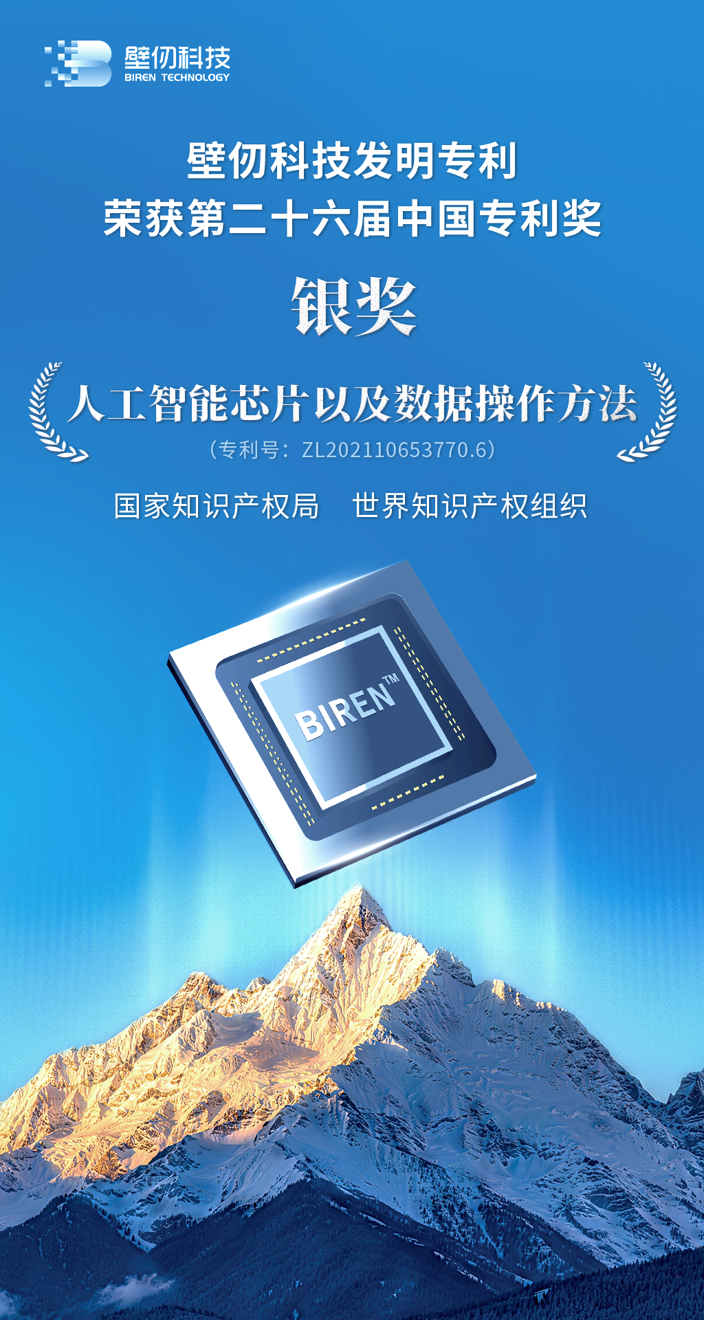
Recently, the China National Intellectual Property Administration (CNIPA) unveiled the winners of the 26th China Patent Award. A core invention patent in the general‑purpose GPU field submitted by Biren Technology, titled Artificial Intelligence Chip and Data Operation Method (Patent No.: ZL202110653770.6), has been honoured with the China Patent Silver Medal.
Jointly presented by the CNIPA and the World Intellectual Property Organization (WIPO), the China Patent Award is China’s sole national‑level award recognising granted patents and represents the highest government‑endowed honour in the domestic patent sector. It aims to reward patent holders and inventors who have made outstanding contributions to innovation implementation and socio‑economic advancement. Winning the China Patent Silver Medal on its very first submission constitutes authoritative validation of the company’s intellectual property achievements and technological superiority, and fully demonstrates Biren’s profound technical expertise and robust architectural innovation capabilities in GPU chip development.
According to official data, the Gold, Silver and Excellence awards of this year’s China Patent Award were selected from invention patents and utility‑model patents, comprising 30 Gold Medals, 59 Silver Medals and 535 Excellence Awards.
【Innovative Computing‑Communication Converged Architecture】
【Breaking the “Communication Wall” Bottleneck of Large‑Model Clusters】
Driven by the rapid evolution of AI technologies represented by large language models, trillion‑parameter models create a critical demand for collaborative computing on GPU clusters with thousands to tens of thousands of cards. Nevertheless, conventional GPU clusters suffer from complex collective‑communication workflows across nodes and insufficient transmission efficiency. Such communication bottlenecks limit the training and inference performance of large‑scale models.
This awarded patent delivers an innovative solution at the chip‑architecture level. By integrating an extended address processor inside the GPU that works in coordination with arithmetic processors, the design effectively cuts down cross‑node data‑transfer steps and achieves deep convergence between computation and communication. When running large‑model training workloads, GPU clusters built on this innovation can notably reduce communication latency and substantially boost data‑throughput performance and overall computing efficiency.
Notably, the patent titled Artificial Intelligence Chip and Data Operation Method was originally filed in April 2021. At an early stage of industrial development, Biren Technology foresaw the trend for AI cluster computing and captured the pivotal value of compute‑communication convergence for cluster efficiency gains. Building on this technical direction, the company has secured a global portfolio of dozens of patents, of which this award‑winning patent stands as a core representative.
【Leveraging Full‑Stack In‑House R&D Capabilities】
【Consolidating the Foundation for Independent Innovation】
Biren Technology brings together nearly 1,000 top‑tier talents worldwide and has built robust proprietary technologies and engineering capabilities. The company has twice won the SAIL Award, the highest honour at the World Artificial Intelligence Conference, and been recognised as a national key “Little Giant” specialised‑and‑sophisticated enterprise.
As of the end of June 2026, the company had filed 1,917 patent applications globally, ranking among China’s top domestic general‑purpose GPU vendors. It holds 1,006 granted patents worldwide, the highest figure among Chinese general‑purpose GPU firms, with a 100% grant rate for invention patents, leading domestic chip companies.
Biren is accredited as a National Intellectual Property Advantage Enterprise and a Shanghai‑level patent pilot enterprise. Two of its core trademarks are included on Shanghai’s key trademark protection list. The company has also obtained certification for the national intellectual property management system, and its jointly submitted project on “chiplet interconnection” has been selected for a special research programme administered by the China National Intellectual Property Administration.
As a domestic leader in general‑purpose GPUs, Biren Technology has always positioned Innovation as the core driver of its RECIPE corporate culture. Looking ahead, the firm will continue to scale up R&D investment, foster deep integration of technological and industrial innovation, and collaborate with upstream and downstream partners across the supply chain. It aims to advance the self‑reliant and controllable development of China’s computing‑power industry and deliver robust chip‑driven momentum for China’s digital economy and artificial‑intelligence sector.
 Jumbo Sheen Fund
Disclaimer:The content involved in this article is for sharing and exchange purposes only, and shall not be construed as investment advice. It is provided merely for readers' reference. All copyrights of the quoted content belong to the original authors. If any infringement is found, please contact us for removal.